
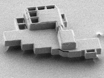
silicon. dimensions: 60 x 80 x 10 micrometers.
A 1/1 millionth scale model of Frank Lloyd Wright's Fallingwater, fabricated from silicon using ultra high precision lithography.
silicon. dimensions: 60 x 80 x 10 micrometers.
A 1/1 millionth scale model of Frank Lloyd Wright's Fallingwater, fabricated from silicon using ultra high precision lithography.
courtesy catharine clark gallery, san francisco, ca.
``Although the senses occasionally mislead us respecting minute objects, such as are so far removed from us as to be beyond the reach of close observation, there are yet many other of their informations, the truth of which it is manifestly impossible to doubt; as for example, that I am in this place, seated by the fire, clothed in a winter dressing gown, and that I hold in my hands this piece of paper....'' Descartes, Meditations.
Why Fallingwater?
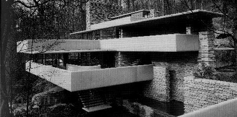
Wright employed the
cantilever:
a horizontal structure for distributing force,
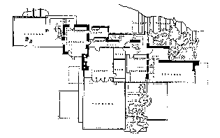
(L) Frank Lloyd Wright's floorplan. (R) CAD model.
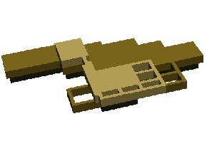
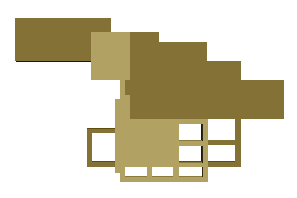
CAD model
How it was made:
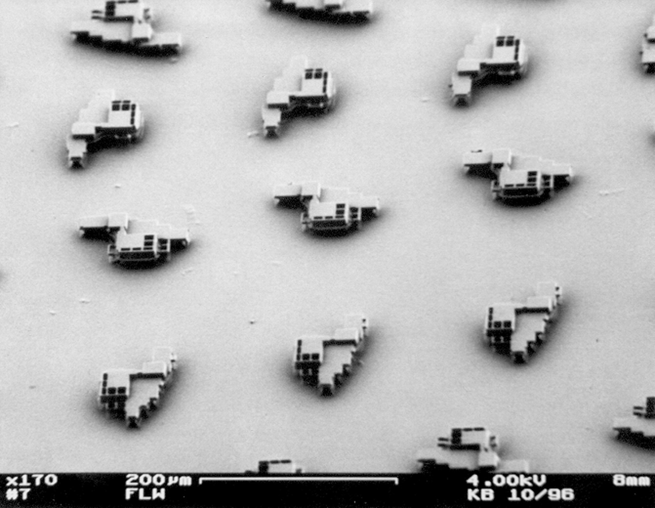
The flw silicon 3D structure was fabricated using a process known as SCREAM, Single Crystal Reactive Etching And Metallization. The process began by scanning in Frank Lloyd Wright's floorplans from a book. These are then imported into a software package that we use to generate a proportional but simplified 3D model of the building with its cantilevered balconies. This model is then used by the computer to create a sequence of optical masks. Note: the structure is so small that 48 copies fit comfortably into a region the size of a peppercorn.
Once the masks are ready, a wafer of purified silicon is treated with a light-sensitive chemical known as photo-resist. In a clean room laboratory, the masks are then used to expose selected areas of the wafer to ultraviolet light, which renders the photoresist susceptible to dissolving in a developer solution. The first mask corresponds to the top floor of the building.
The exposed areas of the wafer are washed clean with deionized water, and then a reactive ion etch is applied to the wafer. The etch occurs in a vacuum chamber where chlorine radicals are accelerated by electrostatic fields during a plasma discharge. The ions remove the silicon in unprotected areas, leaving only the patterns defined by the photoresist. The etch cuts deep into the bulk silicon, creating 3-dimensional structures.
The lithographic procedure is then repeated with the next mask, etching downward from the top floor to each lower floor. Each etching procedure takes several hours including the lithography and cleaning steps. A final plasma etch with sulfur-fluoride ions is used to undercut the silicon, creating the suspended cantilevers in 48 copies of the completed structures.
Exhibition History: